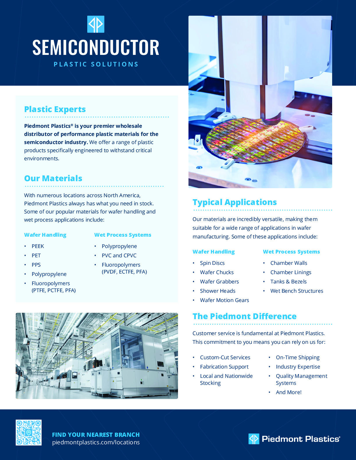
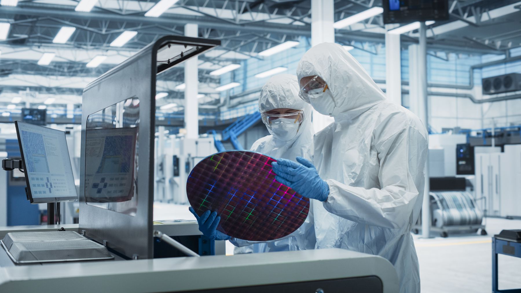
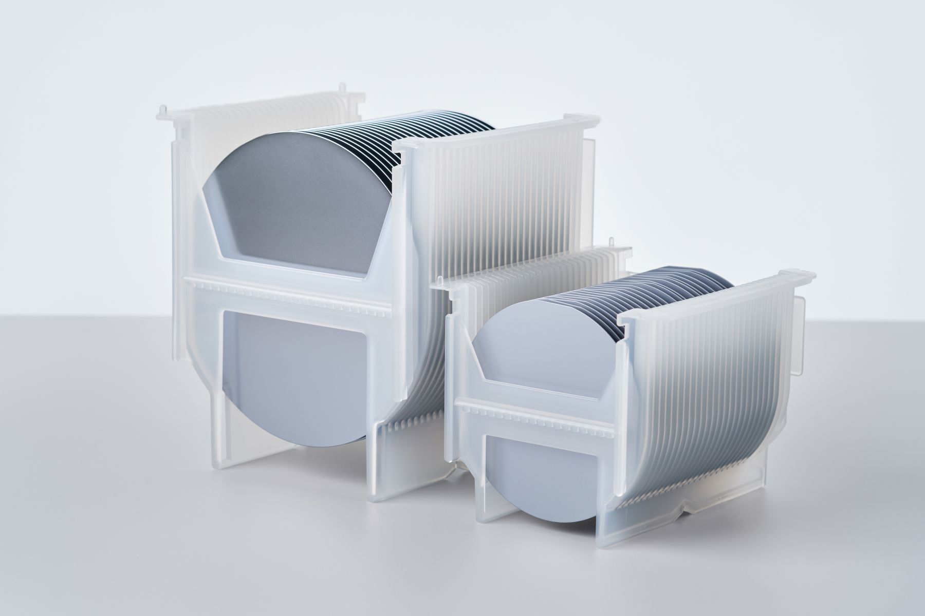
Wafer processing is a term used to describe the process of creating chips, or integrated circuits, that are present in everyday electrical and electronic devices. High quality thermoplastics play an integral role in this process due to their unique characteristics. Because of its outstanding combination of physical properties, PEEK (polyether ether ketone) has been a material of choice for semiconductor wafer processing applications including structural parts in electronics and telecom equipment and integrated circuit (IC) test sockets. PEEK exhibits low moisture absorption and high chemical-, wear-, and thermal-resistance properties. PEEK also displays good management of static electricity.
The Semitron® line of semiconductor grade products maintains the same superior qualities of PEEK while providing increased strength, dimensional stability, and machinability. Semitron® outperforms other materials in its longevity and value compared to other engineering materials.
Piedmont Plastics stocks a variety of PEEK and Semitron® products engineered to optimize the precision performance of device manufacturing equipment. Our knowledgeable representatives will guide you in selecting the best materials for your semiconductor industry needs.

Semiconductor Wafers
Thermoplastics are important in wafer processing. Piedmont Plastics offers polyether ether ketone (PEEK), which works well in electronics and telecom equipment manufacturing. Shop for this and other semiconductor materials.


Related Articles
Plastics in Wafer Processing
High-performance plastics enable clean and reliable wafer manufacturing with ...
The Role of ESD-Safe Plastics in Semiconductor Wafer Carriers
Learn how ESD-safe plastics ensure protection, precision, and purity in ...

Which Plastics Work Best in Semiconductor Manufacturing Applications?
A Q&A guide explaining which plastics perform best in semiconductor ...
Common Industries

Semiconductor
Piedmont Plastics supplies high-performance plastics for the semiconductor ...
Talk to An Expert In
Columbus
460 Schrock Road
614-985-0745